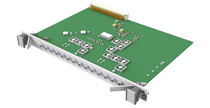
Quantum Computing RF Interface
Designed a complete Quantum Computing RF interface with very high gain modulators and demodulators, flat response up to 12 GHz high power RF PA, down-conversion and filters, and ultralow noise power with RMS noise voltage levels into nanovolt range. An innovative adaptive calibration circuit design to adjust the operative point of critical RF circuits within 0.5% precision. The stage coordinated a calibration scheme during power-up sequencing and compensated part-to-part variations and manufacturing tolerances. To eliminate any PCB sources of loss, a special PCB stack up was planned capable of 110 GHz operation. Crowded RF pathways with 14 input/output connectors were placed meticulously to minimize any cross-talk and shorten signal pathways. The final actual assembly measurements were on par with the simulation modeling, proving the circuit operated equivalent to an ideal model with no noise added from the power or PCB.


